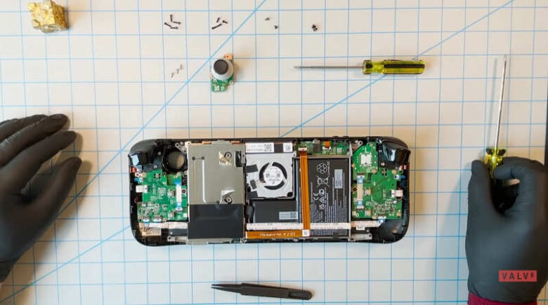
Valve’s much-anticipated Switch-like handheld, the Steam Deck, has officially been revealed, and we have a glimpse at the console’s internal components. Valve has produced an official deconstruction video of its Steam Deck hybrid console demonstrating the components and how to replace some of the more noticeable parts.
In the classic sense, it isn’t a disassembly video. The video mostly demonstrates how to change the thumbsticks and SSD, but it also provides a comprehensive overview of the components. The video also promises to demonstrate why people should not attempt to do this on their own.
So do with that what you will. The video spends some time emphasizing why you should never, ever take the console apart on your own, but we finally get a look inside at the two-minute mark.
The battery is on the right, and an exterior shield protects the SSD and AMD Van Gogh APU on the left. A fan is located in the center, but the remainder of the cooling system (including the heat sink) is located beneath the outer shield. You’ll notice that everything is crammed in close together.
The narrator points out that an off-the-shelf SSD may have an impact on power usage and other components. When the outer shield is removed, we can see what is most likely the APU underneath (though the narrator makes no mention of this).
The APU (AMD’s term for a CPU/GPU combination) is the Steam Deck’s main selling feature. It’s like a supercharged version of integrated graphics. The Xbox One X and PS5 both use the same architecture for their chips. Obviously, the Steam Deck will not be able to match that level of performance. There is simply not enough room for all of the cores. However, early tests have indicated that on the Steam Deck’s 720p display, it provides for a pleasurable gaming experience.
While the Steam Deck won’t win any awards for repairability, it’s always interesting to see what’s going on underneath the hood. Early funders will receive their first Steam Decks in December.


Leave a Reply